Since the arrival of atomically thin graphene, there has been an enormous increase in graphene-based applications in the fields of electronics, chemistry, and mechanics. Over the past decade, various prototypes have been introduced; however, the development of viable electronic devices, the most promising application area, has not met industrial expectations. Despite its many excellent physical properties, including high carrier mobility and superior mechanical strength, graphene has a fatal disadvantage: it is difficult to form a suitable bandgap. An alternative means to resolve this problem is via the engineering of 2-dimensional (2D) materials with suitable bandgaps that can serve as essential components for electronic devices.
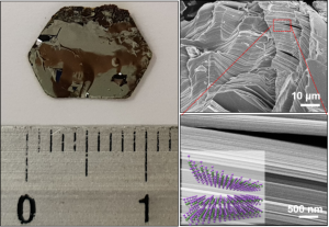
Image of a 1-cm bulk Nb3I8 crystal. Also shown are low- and high-magnification scanning electron microscope images of the Nb3I8 crystal. The inset shows a schematic illustration of the layered crystal structure.
Recent studies by the Nanomaterial Research Lab in SKKU suggest that Nb3X8 (X=Cl, Br, or I),(1, 2), which has strong covalent bonds in the layer plane and a weak van der Waals attraction between layers of 2D sheets, could form one such category of new 2D materials. In particular, theoretical calculations show that monolayer Nb3X8 may have a bandgap with a ferromagnetic characteristic that has not yet been reported in other 2D materials. Unfortunately, to date, experimental studies of Nb3X8 have only evaluated the characteristics of the bulk material, and have not directly explored its layered-structure and changes in physical properties with respect to the number of layers.
Here, a centimeter-sized Nb3I8 crystal was synthesized by a facile vapor transport reaction. As in the case of graphene, via mechanical exfoliation (the famous “Scotch tape” method), a few-layers, or even monolayer, of Nb3I8 flakes were successfully separated from a bulk Nb3I8 crystal consisting of numerous monolayers of Nb3I8 connected by weak van der Waals interaction. By utilizing atomic force microscopy and scanning Kelvin probe microscopy, they observed a variation in work function of Nb3I8 flakes that is thickness dependent.
Prof. Jae-Hyun Lee and Prof. Jae-Young Choi say that “beginning with this research, we are exploring veiled 2D layered materials as well as 0-dimensional and 1-dimensional layered materials to realize 2D heterostructures by a bottom-up approach.”