Electronic memories have played a key role promoting humanity’s progress during the last four decades. Thanks to their ability of storing and processing large amounts of information in ultra-reduced spaces, memory devices allowed the design of super powerful working tools, and created plenty of new services and jobs. The most successful memory device ever designed is the NAND Flash, a technology that has almost monopolized the memory market since its first commercialization in 1989. Now, after more than a quarter-century of aggressive scaling down, a disruptive new family of memories, called resistive random access memories (ReRAM), may overcome the performance of the NAND flash in terms of switching speed, power consumption, data retention, cycling endurance, scalability, 3D integration capability and even fabrication costs. ReRAM devices store information by tuning the electrical resistance of an insulating film sandwiched by two electrodes. By applying controlled electronic stresses, two logic states (the high resistive state and the low resistive) can be cyclically induced. Nevertheless, studying the physical origin of the resistive switching is extremely complex, as it is a local phenomenon that usually takes place is areas of just few nanometers.
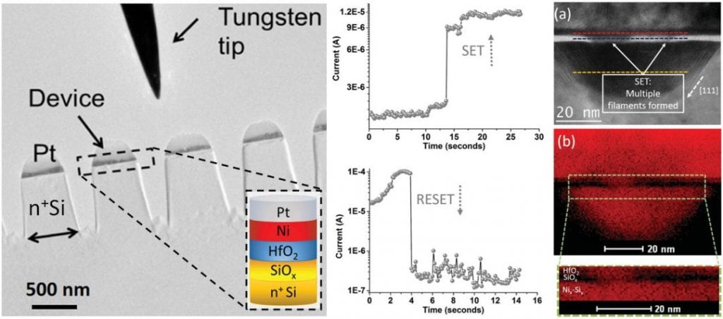
Professor Kin Leong Pey (from Singapore University of Technology and Design) and co-workers have recently presented a revolutionary approach for in-situ visualization of resistive switching. Electrode/insulator/electrode stack blankets were processed via focused ion beam to produce a thin membrane with multiple nanopillars, which served as independent memory cells. This structure is then transferred onto a grounded transmission electron microscope (TEM) copper grid, and an ultra sharp metallic tip is placed directly on the top electrodes of each cell. Using an external semiconductor parameter analyzer connected to the tip, each memory cell can be set and reset while the morphology and chemical composition of the sample is simultaneously imaged via TEM coupled with energy dispersive X-ray spectrometry (EDX) and electron energy loss spectroscopy (EELS).
In their Advanced Electronic Materials paper, it is found that the resistive switching in Ni/HfO2/SiOX/n+Si ReRAM devices is driven by the diffusion of Ni though the HfO2/SiOX dielectric stack, rather than by oxygen vacancies migration, as it was previously believed. These experiments were performed at the extraordinary laboratories of the King Abdullah University of Science and Technology, in collaboration with professor Xixiang Zhang. Due to the unusual clarity of the results presented and thanks to the possibility of collecting electrical, morphological and chemical information at the same time, this methodology may mark a before and after in the study of resistive switching memory devices.