Organohalide lead perovskites (CH3NH3PbI3) have recently received extensive attention for their applications as high-performance low-cost photovoltaic devices, including solar cells and visible light photodetectors. For example, perovskite phototransistors are capable of achieving a photoresponsivity (320 A/W), ranking among the highest values ever reported. They are highly absorptive and represent a direct band-gap semiconductor (1.6 eV) with high carrier mobilities.
In their recent paper published in Physica Status Solidi A: Applications and Materials Science, Alex Zakhidov et al. (Texas State University, USA) have demonstrated a high-resolution patterning technique to obtain CH3NH3PbI3 thin films based on orthogonal lithography. They have used hydrofluoroether (HFE) solvents that are chemically orthogonal to perovskite thin films and do not adversely affect the stability of the films. The patterning process starts with the deposition of a transport layer onto an ITO/glass slide substrate. After growing the perovskite film, spin coating of a fluorbased photoresist, selective UV light exposure, and developing the resist in HFE, the pattern is transferred to the perovskite film via reactive ion etch (RIE).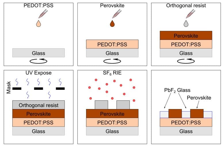
The exposed parts of the perovskite film are transformed into PbF2 which furnishes the functionalized perovskite films after removing the resist. Here, the authors have a process at hand which minimizes cross-talk between neighboring perovskite photodetectors (pixels) while maintaining acceptable efficiencies. This interesting patterning of organohalide lead perovskites may facilitate further progress of technological and industrial processes. The researchers further believe that this method is useful for the simple monolithic integration of perovskite photodiodes to the silicon backplane chip utilized in active-pixel sensor and charge-coupled device applications.