A new solar cell is described that relies on a thin layer of clean CdS, in which a high-field domain extracts holes from p-type emitters without having pn-junctions involved. This design is highly advantageous for increasing the efficiency of the solar cell significantly, by avoiding junction leakage and by increasing the open circuit voltage to its theoretical value approaching the band gap at T = 0 K.
Based on long discussions with Rommel Noufi, I learned only a few months ago that we did the analysis of solar cells simply wrong. I connected the solar current in CuxS with the diode equation in CdS and received jV characteristics that with a few adjustable parameters did fit the measure characteristics. This was too simplified and we lost all the important ingredients.
So I tried to develop a new solar cell theory that is based on experimental evidence, only without using tabulated values like electron affinities and work functions, and relying only on directly measured (and not derived) values. That yielded the first to scale model of the CdS/CdTe solar cell that is given in the next section.
The new solar cell model
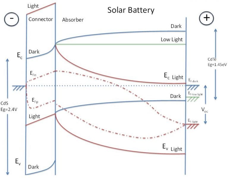
The suggested model shown in the figure is based on the measured values of a typical CdS/CdTe solar cell.
The entire solar cell operation is controlled by the minimum entropy principle that translates into a simple equation dj/dV = 0.
The general cause is the solar energy input that shifts the quasi-Fermi levels down and creates the diffusion current from the gradient of EFp (x) with a minimum close to the center of the CdTe (since there is some loss because of recombination at the electrode to CdTe). The amount of shift and hence the voltage at the operational point is now determined by the minimum entropy condition that must include the external circuit. The band distribution is more difficult to understand and adjusts automatically. It is shown schematically for three cases in the figure.
It is very important to realize that in the dark the electron currents connect at the CdS/CdTe interface, while in the light the hole current connects causing a very large shift of the interface dipole moment and a major shift of the edge connection. This is the reason why back flux of electrons in the operating cell is suppressed and consequently junction leakage is stopped and the open circuit voltage can approach its theoretical limit.
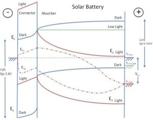 A band model of the CdS/CdTe solar cell[1] under different operating conditions: dark, low light excitation where by extrapolation the bands are flat (shown as thin line for the conduction band), and AM1 at maximum power point, is shown in the figure. It shows the Fermi level in the dark (thermodynamic equilibrium) and the quasi-Fermi levels for electrons (schematically) and for holes (to indicate the photoelectric current) in steady state. At the left is the thin layer of clean CdS that shows a high- field domain[2] that extracts the holes from the CdTe and lets them tunnel into the base electrode at the left of CdS.
The CdS is passive and therefore the Fermi-level at its electrode remains unchanged. It is therefore important for increasing Voc of the solar cell, to dope the CdS with shallow donors in a thin layer near the surface, which may be achieved by washing the surface onto which the CdS is deposited with a gallium containing compound solution.
Consequences for the Si and III-V compound solar cells
Similar features are expected when a thin clean layer of CdS is attached (patents pending in China, USA, and Europe) to a Si or III-V compound solar cell that have no pn-junction. If applied properly, for instance by liquid solution epitaxy for a hydrazene bath, as well described in the literature. Since hydrazene may leach out some elements from the III-V compound, one may introduce a thin hole permeable blocking layer in between. The layer is kept thin to avoid series resistance limitation, so one expects major increases in the cell efficiency because junction leakage is omitted (there is no more junction!). In order to keep the CdS thin before pinholes appear one has to trick crystal growth from a planar (cleaved?) surface with many nucleation sites close to each other, because CdS grows c-axis up with very large crystallization speed. Closeness of nucleation would give the horizontal growth time to fill-in possible pinholes.
Gratitude
I’d like to express my gratitude to Rommel Noufi who has pointed out by referring to a large amount of experimental results that we took a too simplified approach to explain all of that, and to Steward Boden who wrote to me that he and his colleagues were trying to get rid of the pn-junctions in Si and III-V compounds.
References
[1] K. W. Böer, “A new solar cell from a clean cds as connector to a p-type collector without a pn-junction and the minimum entropy principle permits achieving maximum efficiency”, Journal of Applied Physics (2016, submitted).
[2] K. W. Böer, “The importance of gold-electrode-adjacent stationary high-field Böer domains for the photoconductivity of CdS”, Annalen der Physik 527, 378–395 (2015).

