Materials so thin they are considered two dimensional are only a couple atoms thick and, at this scale, they behave in surprising ways. Graphene, for example, is ultrathin graphite, the same material used in pencils. But once sliced to a nanosized thickness, it becomes stronger than steel by weight and is among the best materials for conducting electricity.
As with graphene and many other 2D materials, the same attribute that makes them so attractive — their thickness — is also holding back large-scale production. That’s because 2D materials are fragile and prone to damage when researchers attempt to move them or use them in a device.
To overcome this and unlock 2D materials’ potential for commercial production, researchers have recently developed a “molecular tape” that gently adheres to ultrathin materials and selectively releases them exactly where needed using only UV light.
Promising materials that remain stuck in the lab
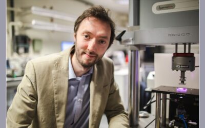
“The variety of 2D materials has vastly increased since the isolation of graphene in 2004, with materials covering the whole range of electronic and magnetic properties,” explained Hiroki Ago, professor at Kyushu University and lead author of the study, published in Nature Electronics, describing the new adhesive.
Ago’s lab has spent 10 years developing synthesis techniques for a variety of 2D materials, like high quality graphene and metal 2D semiconductors. “Many researchers requested our samples, but most of them had problems transferring these 2D materials to their substrates,” he explained. “Due to the thin and delicate nature of 2D materials it is very difficult to transfer them for scientific research and industrial applications,” he said, meaning many promising materials are stuck in the labs where they are produced.
“Therefore, I thought if they can easily transfer 2D materials onto their specific substrates by themselves, 2D materials research and applications will be strongly boosted,” said Ago.
Controlling stickiness
To make the tape user-friendly and simple, Ago and his colleagues devised a material that could selectively stick and un-stick to the 2D materials using UV light. This reduces the chance for damage to occur when the 2D materials are transferred from one surface and to another.
The base of the new tape is a thin layer made from a plastic polymer which gives the tape enough rigidity to be stable and enough flexibility to not damage the materials during transport. Next comes a special blend of polymers — long, chain-like structures made from repeating molecules — that safely attaches to the 2D materials.
“When first adhered to the 2D material, the adhesive layer is soft enough, enabling a uniform contact with the surface and facilitating a full transfer,” Ago said.
Within this adhesive blend, however, are some UV-sensitive polymers which, when exposed to UV light, crosslink, meaning they form a series of repeating, tight bonds throughout the polymer, hardening the adhesive layer. As the tape hardens, it cleanly detaches from and releases the 2D material without the need for destructive manual or chemical processing to remove the tape.
Better than expected performance
By manipulating the composition of the polymers in the adhesive, the team could fine tune stickiness and release of the tape for a variety of different 2D materials. “This adaptability ensures the versatility of the UV tapes and their potential in a broad range of applications,” Ago said.
Tests showed the tape greatly reduced the amount of residue and cleaning required after transfer and produced more uniform transfers with fewer cracks when compared to standard methods. “And it allowed for the transfer of larger areas up to the size of 4-inche wafers, which is essential for the adoption of 2D materials at industrial scales,” Ago said.
The tape surprised everyone though when the team tested scenarios beyond their initial designs. It proved successful when transferring 2D materials to fragile or curved surfaces, and the team was able to precisely layer different 2D materials together. Mixing and matching layers and controlling the angles between them, known as twist angles, can significantly boost electrical properties, leading to superconductive states for example.
The team also showed that they could easily cut the tape and transfer different shapes and sizes, enabling researchers to selectively transfer and position custom sized 2D sheets quite easily. This ability to customize should reduce the amount of adhesive needed and further lower production costs for industry.
The team is now working to improve the composition of the adhesive layer as there is still some wrinkling and bubbling occurring. Efforts are also being made to scale up the sizes, and to one day transfer patterned 2D materials.
Reference: Hiroki Ago, et al. Ready-to-transfer two-dimensional materials using tunable adhesive force tapes, Nature Electronics (2024). DOI: 10.1038/s41928-024-01121-3
Feature image credit: Hiroki Ago et al. Nat Electron (2024)