 Due to their unique optical and electrical properties, conjugated polymers (CPs) are being investigated for a wide range of applications including light emitting diodes (LEDs), photovoltaics, sensors, and transistors. In order to incorporate CPs into next generation devices, cost effective methods are needed to pattern the active materials over large areas. Photolithography, the predominant method for creating silicon micro-electronics, is an obvious choice; however, challenges remain in utilizing the technique for patterning active organic materials. Typical approaches to photopatterning CP’s include functionalizing the polymers with photo-active groups that eliminate upon UV exposure, causing a decrease in solubility; unexposed areas are removed by dissolution in a solvent forming a pattern (negative tone resist). One of the main draw-backs to this approach is that the polymers are exposed to UV light, which can degrade the electrical and optical properties of the active material.
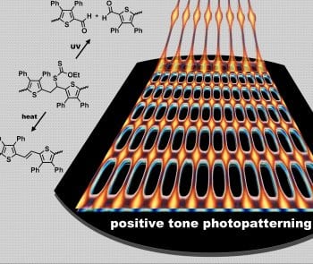
A new approach is now described that takes advantage of UV degradation to increase the solubility of the exposed areas (a positive tone resist); the unexposed regions remain after the developing step, and form a pattern without being subjected to UV light. It is shown that a precursor to a poly(thienylene vinylene) analogue, a low band-gap CP with unique electrical and optical properties, efficiently photopatterns as a positive tone resist. The photochemistry behind the result is investigated, and it is shown that photo-oxidative chain-scission of the polymer backbone reduces the molecular weight of the exposed areas, allowing for selective dissolution. The patterning technique is efficient, scalable, capable of single micron resolution, and should be applicable to alternate classes of CPs; most importantly, the active material is patterned without degradation to its properties.


