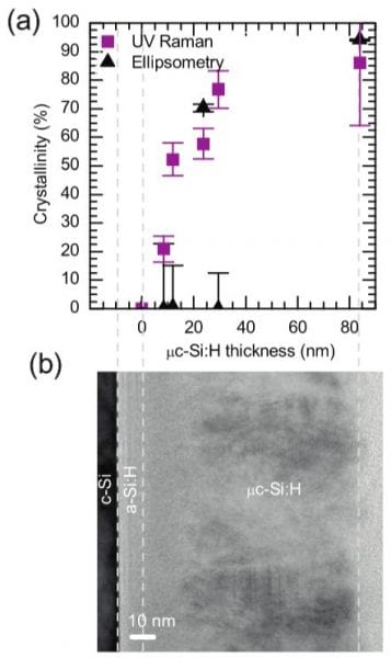
(a) Crystallinity, as determined from UV Raman and ellipsometry, of microcrystalline silicon films 0–84 nm thick on 10 nm of amorphous silicon on silicon wafers. The ellipsometry crystallinity is the percent of polycrystalline silicon in the effective medium approximation used to model the microcrystalline silicon film. Crystallinity error bars represent 90% confidence intervals of the fits; the thickness error is <1 nm for all measurements and is not shown. (b) Bright-field transmission electron micrograph of the thickest (84 nm) microcrystalline silicon film. The microcrystalline silicon, amorphous silicon, and wafer surfaces are demarcated with dashed lines.
Analyzing the surface, and only the surface, with light, of devices with nanoscale layers, such as microchips, sensors, and solar cells, becomes challenging.
One method for analysis is Raman spectroscopy, which gives a “fingerprint” of a material, but tends to give bulk properties with the commonly used green laser sources. For example, Raman spectra can be used to calculate the crystallinity of a silicon film, which reveals information about the optical and electrical properties of the film. However, if the film is thin and deposited on a silicon substrate, its signal cannot easily be deconvoluted from the underlying layer.
In a recently published article in Physica Status Solidi B, scientists from the US have demonstrated that UV Raman spectroscopy can be used to analyze the crystallinity of silicon films as thin as 13 nm. If the thin film has the same thickness as the Raman collection depth, a characteristic depth commonly used in Raman analysis, then too much signal from the bulk is collected to properly analyze the surface, as confirmed by measurements of ultrathin amorphous silicon layers on silicon substrates.
The authors defined a new characteristic depth, the Raman detection thickness, which is the thickness from which the signal collected from the substrate is only 5% of what it would be in the absence of an overlaying film. The 325-nm excitation used for UV Raman spectroscopy has a Raman detection thickness of only 13 nm within the silicon thin film, thus eliminating signal from the substrate.
The UV Raman spectroscopy approach is particularly useful for layers grown on substrates of the same material but with different microstructure, and can be extended to non-silicon materials, particularly nanocrystalline solids.
The text was kindly provided by Joe Carpenter, and edited by Ekatarina Perets. Image credit: Georgy Shafeev/Shutterstock