Cuprous oxide (Cu2O) is a low-cost, nontoxic semiconductor material regarded as one of the most promising semiconducting oxides available for photovoltaic (PV) applications. This is mainly attributed to its good absorption coefficient for visible light, resulting in a high PV conversion efficiency. Despite its significant advantages over other materials, its successful cost-effective transformation into solar panels remains a challenge. One major reason for this is the lack of processing methods that will result in defect-free PVs.
Over the past few years, researchers have experimented with various deposition methods in an effort to tackle this issue. Among them, sputtering has gained significant attention as a widely used low-cost manufacturing process that is promising for PV applications. The technique is governed by the ejection of atoms from a solid target material due to bombardment of the target by high energy particles. Layer by layer the ejected atoms are deposited as a thin film onto a substrate across the target material. A significant drawback that has undercut its success in PVs, however, has been the inferior crystallinity of the obtained Cu2O film and the occasional damage of the underlying substrate, conditions that are detrimental for the operation of the solar cell.
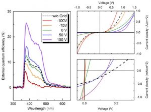
In a recent study in Physica Status Solid A: Applications and Materials Science, Professor Slobodan Mitic and co-authors from Justus-Liebig-Universität in Germany showed that when a biased semi-transparent electrode is introduced between the target and the film the Cu2O morphology can be modified by the electron temperature in the plasma. Controlling the electron temperature allowed them to tune the plasma reaction by reducing the amount of ionized particles that disturb it. The group showed that if the ion energy is sufficiently reduced, the film’s stoichiometry can be carefully tuned to improve its PV efficiency, showing that sputtering can be successfully used as a fabrication process of such films. “The semi-transparent grid at positive bias reduces the ion energies and, therefore, the interface damage, resulting in lower defect density […]. This improves the performance of the solar cell […] rendering the low-cost process of sputtering a highly competitive fabrication method for PVs”, they said.