Researchers create junctions, essential to electronics fabrication, by transferring graphene films onto patterned monolayer substrates.
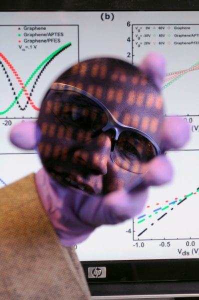
Researchers create junctions, essential to electronics fabrication, by transferring graphene films onto patterned monolayer substrates.
Electronics coating firm expands business in Turkey, Qatar, the United Arab Emirates and Saudi Arabia.
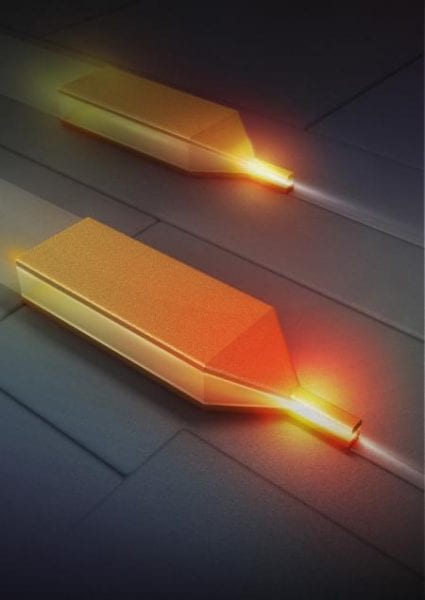
Engineers create a device that can focus light into a point of just a few nanometers, with applications in computing, communications, and imaging.
A state-of-the-art welding process refined for use in naval shipbuilding by the Office of Naval Research (ONR) has crossed over to the world of computing.
New galvanisation process from Fraunhofer Institute for Microelectronic Circuits and Systems IMS offers promise of better LEDs.
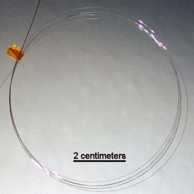
Researchers make a fiber out of crystalline silicon semiconductor materials that can function as a solar cell.
ICOS WI-2280 designed specifically for defect inspection and 2D metrology for LED applications.
Purdue and Harvard researchers create stackable indium-gallium-arsenide transistors.
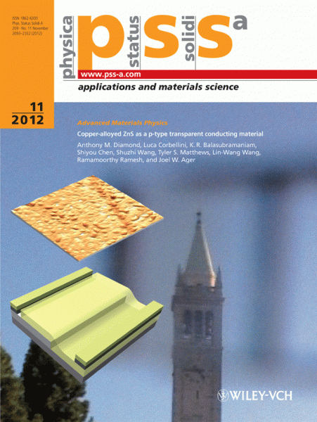
Researchers have developed a transparent diode with copper-alloyed zinc sulfide as p-type conducting material.
Veeco announces multiple metal organic chemical vapor deposition orders from Deli Optoelectronics, of Guangdong, China.
 Titanium-based metamaterial unlocks strength beyond nature
 An anti-inflammatory peptide may hold the key to low-back pain relief
 Materialism matters: The role of philosophy in science
 Researchers uncover a fundamental driver behind osteoarthritis
 Ibuprofen’s effect on red blood cells: A prickly affair
 Quantum entanglement visualized for the first time ever
 The dramatic story behind general relativity’s Nobel Prize snub
 How the brain protects itself from the negative effects of CBD
 First ever diagnostic test for chronic fatigue syndrome sparks hope
 New anti-aging ingredient pulled from medicinal herb