 Very small organic thin-film transistors with high operating frequencies have been produced by Japanese and German scientists.
Organic thin-film transistors (OTFTs) are interesting for electronic applications on flexible plastic substrates, such as rollable or foldable active-matrix displays, conformable sensor arrays, and flexible identification tags. These can be used to make anything from flexible roll-out portable screens to field diagnosis kits and stock labels. The maximum frequency at which OTFTs can be operated is usually limited to about 1 MHz, and for some applications like high-resolution active-matrix displays or flexible sensor arrays, organic TFTs that can be operated at higher frequencies (more than 10 MHz) are needed.
The maximum operation frequency arises because of the relatively slow speed at which electronic and electric currents are able to move through most conjugated organic semiconductors. Higher operation frequencies can be reached if the OTFTs are sufficiently small in the lateral (planar) directions, but this comes at the cost of many disadvantages arising from their small size. The contact resistance (resistance arising from the connections) is also of great importance, as the amount of resistance must scale with size to retain the desirable OTFT properties.
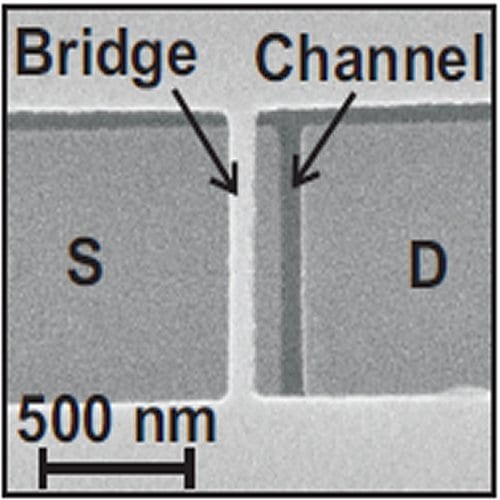
A collaboration between German scientists at the Max Planck Institute for Solid-State Research, Stuttgart, and Novaled AG, Dresden, and Japanese scientists at Hiroshima University, University of Tokyo, and Nippon Kayaku Co., Tokyo, has made a breakthrough to produce very small OTFTs with excellent properties.
In particular, they used an ultrathin gate dielectric based on a molecular self-assembled monolayer. The gate dielectric is the material used to make the terminal of the OTFT and its electrical behavior can be switched by the presence of an electric field, making it a vital part of the OTFT. The scientists also incorporated a strong organic dopant into the contact regions that enabled them to reach the desired levels of contact resistance. This combination of concepts enabled them to demonstrate the first submicron organic transistors with excellent current-voltage characteristics and a record transconductance (approximately, the ratio of the output current to the input voltage), which theoretically corresponds to a maximum operation frequency of over 10 MHz and would thus meet the needs of the high-operating-frequency applications described above.
In the future the scientists hope that their techniques will be helpful in understanding the materials requirements for gate dielectrics and contact dopants to make new and better OTFTs. They do note, however, that the method they use to pattern the substrates, e-beam lithography, is not compatible with a scale-up to large-area electronics. This incompatibility means that, while this method can be used to study and optimize devices, commercial devices could not be made in this way and must be produced using high-resolution printing techniques when these become more routine. Take heed, surface-printing specialists, the challenge is made!


